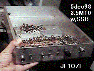
3.5MHz 10W SSB transceiver with 14 transistors:3.5mssbph.gif
 In
every weekend, I go to the top of the mountain and make local expedition
with 50MHz SSB. In week day , after job, I operate 7MHz CW on my shack.
But in these days, on the 7MHz , my signal skips out from Japan and I can
not contact any station after 10 o*clock. Therefore I decided to make 3.5MHz
SSB and CW rigs. I will show you my SSB rig on this page and I will show
you CW one on the next page. With each gears, I could contact about ten
domestic stations.
In
every weekend, I go to the top of the mountain and make local expedition
with 50MHz SSB. In week day , after job, I operate 7MHz CW on my shack.
But in these days, on the 7MHz , my signal skips out from Japan and I can
not contact any station after 10 o*clock. Therefore I decided to make 3.5MHz
SSB and CW rigs. I will show you my SSB rig on this page and I will show
you CW one on the next page. With each gears, I could contact about ten
domestic stations.
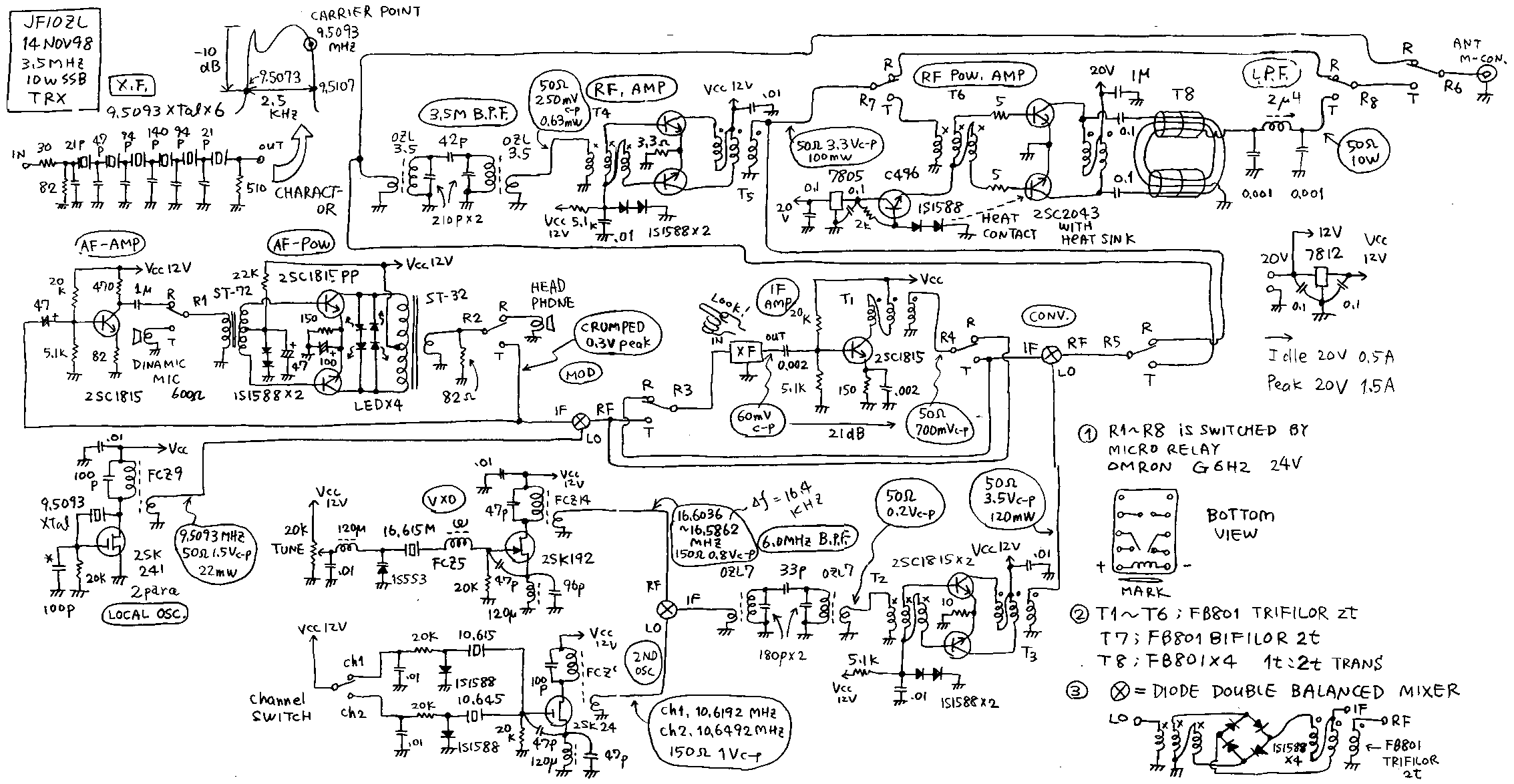
Frequency planning
I have about five hundred*s of crystals on my junk box. On these crystals
, I have some kind of groups that has the same named frequency. With the
same named crystals, I can construct rudder filters and carrier oscillator.
On this case I choose seven 9.50923MHz crystals. With six of them I made
a filter. Band width of it is adjusted for 2.5kHz by changing the capacitors,
by cut and try method. The frequency of the carrier oscillator is adjusted
on the upper edge of the pass band of the filter, by changing the capacitor
on the gate of the oscillator FET, with cut and try method. See the upper
left side of the circuit diagram! Pass band of the filter is from 9.5073
to 9.5107MHz. the carrier frequency is 9.5093MHz. These experiment must
be done before beginning to making the transceiver. On this time I could
get the prospect to make a 9.5093MHz LSB generator. On the next step, I
had to consider how I can convert this 9.5093MHz LSB signal to 3.5MHz LSB
signal. Yes I need 6MHz local oscillator. 9.5MHz LSB-6MHzCW=3.5MHzLSB.
But 6MHz VXO(variable crystal oscillator) can be changed it's frequency
only 12kHz, because VXO can be changed it's frequency about 0.2% of it's
oscillating frequency. 6MHz*0.002=12kHz. In Japan , 3.5MHz SSB band is
from 3.5025 to 3.5075MHz. It*s band width is 50kHz. Therefore this VXO
will be able to cover only a part of the SSB band. I feel it is not good.
In order to make big width VXO, I made 16.165MHz VXO. And I made another
10.615MHz crystal oscillator. And I got 6MHz local signal by subtracting
these two signals. And by changing oscillating frequency of the OX, I can
make two channel of signals. I will put these frequency planning in order
as follows.
"Fcar" is carrier frequency,9.5093MHz.
"Fxvo" is XVO frequency, from 16.6036 to 16.5862MHz.
"Fxo1" is first channel frequency, 10.61902.
"Fxo2" is second channel frequency, 10.64902.
Fout1=Fcer-(Fvxo-Fxo1)=3.5249 to 3.5723
Fout2=Fcer-(Fvxo-Fxo2)=3.5549 to 3.6023
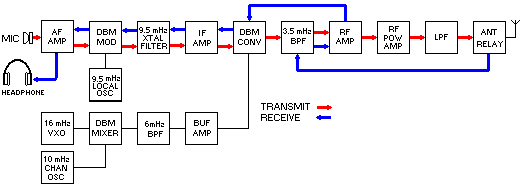
Block diagram
transmitting time
| mic--> |
af amp--> |
DBM-
modulator--> |
9.5M
Xtal filter--> |
IF AMP--> |
DBM-
convertor--> |
3.5M BPF---> |
RF-AMP |
FR-AMP |
LPF |
ANT |
|
9.5MHz-->
local OSC |
upside connect |
|
|
upside connect |
|
|
|
|
|
|
|
|
|
|
upside connect |
|
|
|
|
|
16MHZ
VXO |
-------> |
DBM-
mixer------> |
6MHz
BPF |
Buffer
AMP---> |
upside connect |
|
|
|
|
|
10MHz
XO |
-------> |
upside connect |
|
|
|
|
|
|
|
|
receiving time
| ANT--> |
3.5M BPF---> |
RF amp--> |
RF amp--> |
--> |
DBM-
convertor--> |
9.5M
Xtal filter--> |
IF AMP--> |
DBM-
modulator--> |
af amp--> |
head phone |
|
|
|
|
|
upside connect |
|
9.5MHz-->
local OSC |
upside connect |
|
|
|
|
|
|
|
upside connect |
|
|
|
|
|
16MHZ
VXO |
-------> |
DBM-
mixer------> |
6MHz
BPF |
Buffer
AMP---> |
upside connect |
|
|
|
|
|
10MHz
XO |
-------> |
upside connect |
|
|
|
|
|
|
|
|
Construction and typical point
1. Audio amplifier is a normal transformer input and output type push pull
amplifier. It is used as a microphone amplifier on it*s transmitting time.
It is used as a head phone amplifier on it*s receiving time. On the first
side of the output transformer, the six LED is connected. It limits the
signal strength of the microphone amplifier under 300mVc-p. In order to
avoid distortion, audio signal must be 10dB lower than the carrier signal.
2. On the receiving time , one stage of audio amplifier is pre located
before the push pull amplifier. It can offer the enough total gain of the
receiver. But when I put the capacitor on the emitter of the transistor
this amplifier, the total gain became too much , and my headphone was full
of noises.
3. 120 micro henry of micro inductor is used on the souse of the FET of
the crystal oscillator. I got 1000 pieces of them on these days. Therefore
I decided to use it actively.
4. About crystal filter, please see another page of my home page! The filter
on this transceiver has 6dB ripple on it's pass band. But nobody talked
about my sound on the 3.5MHz SSB because 3.5MHz SSB band is full of noises.
5. In this machine three DBM( double balanced mixer) are used. All are
made with the same parts. 1S1588 switching diodes and FB801 tri-filer transformers
are used. 1S1588 is better than 1N60 on these purpose, because the character
of the silicon diodes are more uniform than germanium diodes. I measured
the carrier suppression of this modulator is better than 40dB.
6. About coils, you can see the name of OZL series and FCZ series. FCZ
series are the mane of the coils made and sold by JH1FCZ. OZL series are
the name of the coils made by myself imitating the FCZ coils. They are
not sold in anywhere in the world. But you can imitate by yourself and
you can use in your original gears. Please see how to make them on the
another page of my home page.
7. T8 is output transformer of the final radio frequency amplifier. T8
is made with four FB801 ferrite beads and 0.2mm diameter poli-uletanne
(enamel) wire. First side of it is winded by one turn. Second side of it
is winded with two turns.
8. Idle current of the final amplifier is 0.3A. In a moment of maximum
power output, the currect of it becomes 2A. Then the power of it becomes
2A*20V=40W. The RF maximum power is 10W. Therefore the final efficiency
is 20%. For our amateurs, that(=20%) is normal numbers. Because input power
of the final amplifier is 40W, I needed very big heat sink. The size of
it must be twice bigger than my perms.
9. Low pass filter after final amplifier is constructed with single pei
filter. The coil of it is winded around the 8mm diameter core bobbin with
0.2mm enamel wire. Only with this simple filter, I did not watch any TVI
on my TV. I felt 3.5MHz is far from TV frequency.
10. Push pull wide band amplifier is used as a driver of the converter.
It has reason. The IF signal on the IF port of the converter DBM becomes
700mVc-p. Therefore the local oscillator signal must be bigger than 2 volts,
to avoid any distortion on this stage. Therefore I used such a high power
amplifier on this stage. Unless this office, some unwanted signal occurs
on convertor DBM and it will happens some TVI or distortion of your voice
signals.
11. I used 1.5D2V slim coxial cables to connect relays and circuits, to
avoid unwanted self oscillation.
12. I like relays. I don't like diode switch. But to change the crystal
of the oscillator in this machine , I used a diode switch. In this case
it works good.
13. I used many 2SC1815 named transistors. It was got by 7 yens per piece.
Yes it is very cheap. But I feel this transistor is almighty on lower HF
small signals. But only on oscillator, I feel the FET has better activity.
14. You can see, the case is very big. It is second use of my uncompleted
FM transceiver. In Japan we have the proverb that bigger is better than
too small.
15. In this machine, it has three oscillators on it. Each load of them
are not changed from transmitting time to receiving time. Therefore the
oscillated frequencies are not changed on it's transmitting time and receiving
time. It is very good point of this construction.
16. In this machine , all small circuits are working as common of transmitter
and receiver. Therefore the useful 10W SSB transceiver is constructed with
only 14 transistors. But this type of construction needs many relays. I
used cheap 24 volt relays with 20 volt power voltage from my regulated
power supply.
17. The Vcc of final is also driven with this 20 volt. Another circuits
are supplied 12 volts by the three legs regulator(7812).
18. I could make contact with all site of Japan by this simple 14 transistor
machine.
19. One time I completed this gear unless the final amplifier. In that
timing, the output power of this transceiver was 100mW. But I could not
make any contact with this machine. I feel the environmental noise will
be bigger than my signal in Japan. In Japan the population is very big.
And we use many electric instruments on the night. The many electric instruments
make many noises. It may be different in your country. You may use this
gear without of final amplifier.
20. I bought a pair of 19 meter long vinyl coated wires. I made a dipole
antenna with them. I set up it around my house very closely on the wall
of my wooden house with bent in some points. Yes it is called bent dipole.
I can not buy the 40 meter long garden , because I am only an employee
of machine company. Full size dipole can be used only farmer or president
of the company in Japan. HIHI
21. From many hand builder living in abroad, untill now, I received many
request to teach them the character of the transistors used on my home
page. Therefore I will show you them below.
2SC1815 : Usage=AF,Type=Si Epi,maker Toshiba,Vcbo=60V,Ic max=150mA,Pc=400mW,ft>80MHz,hfe=100
2SC2043: Usage=RF PA,Type=Si Epi,maker Fujitu,Vcbo=60V,Ic max=8A,Pc=25W,ft=220MHz,hfe=500
2SK241 : Usage=FM VHF,Type=Mos,Maker Toshiba,Vdssmax=20,Idmax=30mA,Pd=200mW,Idss=5mA,gm=10mS
2SK192 : Usage=FM VHF RF,Type=J,Maker Toshiba,Idmax=10mA,Pd=200mW,Idss=10mA,gm=7mS
Operatin in my shack
| date |
time(Japan time) |
call sign |
his RS |
my RS |
his city name |
distance(km from my house) |
| 14Nov98 |
1535 |
JS1DEH |
55 |
55 |
Kanuma city |
65 |
| " |
1701 |
JO1LHC |
59 |
59QRN |
Sano city |
65 |
| " |
1835 |
JH0TFD |
59 |
59 |
Shimotagaigun/Nagano |
190 |
| " |
1855 |
JI2VIF |
59 |
57 |
Inabegun/Mie |
350 |
| 15Nov98 |
2055 |
JR1KJU |
59 |
59 |
Niiharigun-Kasumigaura,town |
10 |
| " |
2218 |
JH7DMM |
59 |
59 |
Futabagun |
170 |
| 16Nov98 |
2150 |
JA2VA |
59 |
18 |
? |
unknown |
| " |
2225 |
JA1VGU |
59 |
39 |
Inbagun,motono,village |
38 |
| 18Nov98 |
2107 |
JA0PE |
59 |
49 |
Kitakanbaragun |
220 |
| " |
2150 |
JQ2LYP |
59 |
59 |
Hizai city/Mie |
380 |
| 19Nov98 |
2307 |
JR3GAL |
59 |
59QRN |
Kusatsu city/Siga |
400 |
3.5mssb.gif
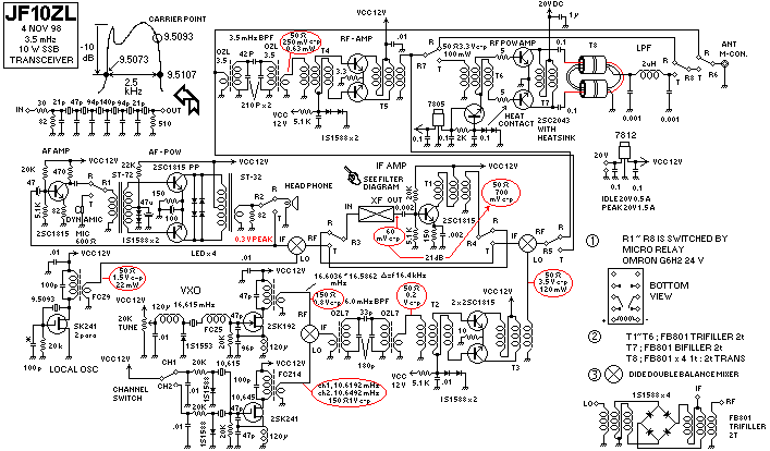
12Feb2000***My internet friend YB0AH prezented these re paint. Thanks!
YB0AHSSBBOLCK.gif
YBAH80MSSB.gif
14石式 3.5MHz 10W SSBトランシーバー:3.5mssbph.gif
私は、週末には、車で山に登って50MHzSSB.平日の夜は、7MHzのCWを中心に運用しています。しかし、近頃は、7MHzのCWを、仕事を終わってから運用しようという頃には、7MHzで国内がスキップしてしまい、思うように交信相手がみつかりません。そこで。一つ下の3.5MHzに降りてみる事にしました。このために、3.5MHzのSSBとCWのトランシーバーを作ってみました。このページでSSBの物を、次のページでCWの物をご紹介します。どちらも数10局交信できました。
周波数計画
私は水晶を500個ぐらい持っています。そのなかで、9から11メガの同じ周波数のものが何種類かあり、そのなかで、今回は9.50923MHzの物を使う事にします。9メガから11メガの水晶は、ラダーでSSB用のフィルターを組むのに適しています。これよりも低い水晶では、どうしても帯域が狭くなってしまいますし、これよりも高い水晶は、どうしても広くなりがちで、無理に狭いものを作ろうとすると、信号の減衰が大きくなってしまいます。さて、9.5093MHZでラダーを組んで、一方同じ水晶で発振器を作ると、どうしても発振周波数が、フィルターの通過帯域の上端になるので、LSBのSSBジェネレーターになります。実際には、下の図の左上の様に、通過帯域が9.5073から9.5107MHzでキャリアポイントを9.5093としました。これだけは、あらかじめバラックでラダーフィルターとキャリア発振器を組んでみて調べます。
そこで、次に、9.5MHzのLSBができましたで、これを3.5MHzのSSBにするのにどうしたら良いかと考えます。3.5MHzはLSBですから、LSBとUSBを反転させないように、6MHzの局部発振器を組み合わせます。すなわち、「9.5MHzLSB−6MHz=3.5MHzLSB」です。3.5MhzのSSBは3.5025MHzから3.5075MHzですので、50kHzのはばがあります。6MHzの発振器をVXOで組んで、これを50kHz動かすと、可変範囲は50k/6M=0.0083すなわち0.8%です。しかし、VXOは一般にいわれる可変範囲は最大で0.5%です。私の経験では、0.2%が安心して使える範囲です。よって、これでは、3.5MHzのSSBバンドのなかの一部分にしか出られませんので、それでも、運用上の不便を割り切ってつかえば良いのですが、今回は「毎晩運用したい」という目的なので、我慢しない事にしました。さりとて、VFOで安定した物を作る自身はありません。そこで、16MHzのVXOと10MHzの水晶発振器を組み合わせて、6MHzの発振器を作りました。あらかじめ2個の発振器から必要な局部
発振器を作っておく事をプリミックス方式といいます。16MHzのVXOは、実際作ってみると16.6036から16.5862MHzまでの16.4KHzの可変範囲でしたので、さらに10MHzの発振器の水晶を名盤周波数で10.615と10.645の二つを切り替えて、2チャンネル化して、合計32.8kHzの可変範囲を得ています。実際の発振周波数は名盤周波数より高くなってそれぞれ、10.6192MHzと10.6492MHzでした。
これまでの話を整理すると、
Fcar=9.5093
Fvxo=from 16.6036 to 16.5862
Fxo1=10.6192
Fxo2=10.6492
Fout1=Fcar−(Fvxo−Fxo1)=3.5249 to 3.5723
Fout2=Fcar−(Fvxo−Fxo2)=3.5549 to 3.6023
となります。
ブロックダイアグラム
送信時
| mic--> |
af amp--> |
DBM-
modulator--> |
9.5M
Xtal filter--> |
IF AMP--> |
DBM-
convertor--> |
3.5M BPF---> |
RF-AMP |
FR-AMP |
LPF |
ANT |
|
9.5MHz-->
local OSC |
upside connect |
|
|
upside connect |
|
|
|
|
|
|
|
|
|
|
upside connect |
|
|
|
|
|
16MHZ
VXO |
-------> |
DBM-
mixer------> |
6MHz
BPF |
Buffer
AMP---> |
upside connect |
|
|
|
|
|
10MHz
XO |
-------> |
upside connect |
|
|
|
|
|
|
|
|
受信時
| ANT--> |
3.5M BPF---> |
RF amp--> |
RF amp--> |
--> |
DBM-
convertor--> |
9.5M
Xtal filter--> |
IF AMP--> |
DBM-
modulator--> |
af amp--> |
head phone |
|
|
|
|
|
upside connect |
|
9.5MHz-->
local OSC |
upside connect |
|
|
|
|
|
|
|
upside connect |
|
|
|
|
|
16MHZ
VXO |
-------> |
DBM-
mixer------> |
6MHz
BPF |
Buffer
AMP---> |
upside connect |
|
|
|
|
|
10MHz
XO |
-------> |
upside connect |
|
|
|
|
|
|
|
|
構成と特徴
1.低周波増幅器は、トランス入出力のプッシュプル増幅器で、出力トランスにLEDを付けて、振幅制限をかけている。これによって、どんなに大きな声でしゃべっても、モジュレーターのDBMには、最大0.3V尖塔値の信号しかはいらない。これで、DBMが飽和して信号が歪むのが避けられる。
2.受信時は低周波増幅器の前に、もう1段低周波増幅器を置いて、利得を稼いで、十分な受信時の総合利得を得ている。エミッターの所にパスコンが入っていないが、これを入れると、増幅率が大きすぎて、ノイズでばりばりいって使えない。
3.VXOのFETのソースの所のコイルは、120マイクロヘンリーのマイクロインダクター。1000個程度入手したので、今回どんどん使う事にした。
4.水晶フィルターに関しては、他のページに詳しくかいてある。今回、作った物は帯域内に6dB程度のリップル(通過損失のあがりさがり)があるが、使ってみると、交信相手は、このバンドでは、どの局もノイズと戦いながらの交信であるので、音質うんぬん言ってくる局は無かった。
5.この器械には、自作のDBMを3個使った。どれも同じ構成。回路図の右下に示した回路である。なんとなく、以前は、モジュレーターは、小さな信号を扱うのだから、ゲルマニウムダイオードを使っていたが、今回は、すべて1S1588というシリコンダイオードをつかった。ゲルマニウムダイオードよりもシルコンダイオードの方が、特性がそろっているせいか、キャリアバランスがよい。もともと、DBMのダイオードは、スイッチング動作をしているのだから、少信号スイッチングダイオードが一番いいのは当たり前である
6.FCZコイルは、JH1FCZさんが作って売っているアマチュア無線用コイル。OZLコイルはこれをまねて作ったもの。他のページをみよ。
7.T8は、FB801のフェライトビーズを4個つかって、これに、0.2mm径のポリウレタン線を1次側は1回、1次側は2回まいた物。
8.ファイナルのアイドル電流は0.3A。最大出力時は、2A*20V。よって、終段入力は40W。これで10W出力なので、効率25%。まあ、こんなもんです。HI。40Wも入力があるので、放熱器は手のひらの2倍の大きさでもかなり暑くなる。
9.LPFはπ型1段。そのコイルは8Φのコア入りボビンに0.2mmのポリウレタン線を14回巻いた物。こんな簡単なLPFでも、TVIは皆無である。さすが、3.5Mはテレビの周波数から遠いと感じますな。
10.プリミクスローカルオッシレーターの出力に、わざわざプッシュプルの緩衝増幅器を入れているのは伊達じゃありません。送信時のIFの信号が、700mVcーpすなわち5mWにもなるので、周波数変換のDBMが飽和しない様に、対向して十分な局発信号をDBMに供給してやる必要がある。これを怠ると、周波数変換段でスプリアスが発生して、音が割れたり、TVIが発生したりする。
11.送受信切り替えのリレーと回路の間の結線はすべて1.5D2Vの細い同軸電線を使って、不要なノイズや、迷結合(製作者の意図しない回路同士の結合)による発振が発生しないようにした。
12.私はリレーが好きで、ダイオードスイッチによる切り替えはあまり好きでない。10MHzの発振器の水晶の切り替えには、ダイオードスイッチを使ってみた。ここではうまくいった。
13.トランジスターは、2SC1815という汎用品を多用している。ft=80MHz,Pc=400mWのこの石は、HFではファイナル以外万能選手である。但し、発振器にはFETの方が、動作の確実安定という点で勝っているようである。偏見かもしれない。
14.ケースは写真を見てお分かりの様に、でかすぎる。以前作った、失敗作の流用である。大は小を兼ねる。
15.3つある発振器全てにとって、その負荷が、送信時と受信時で変わらない。すなわち同じ物がぶらさがっている。これによって、送信時と受信時の周波数がずれる心配が無い。この回路方式の最大の長所である。
16.全段送受信共用の為、すなわちすべての回路が送信時も受信時も働いているので、少ない素子の数で実用的な10WのSSBトランシーバーができる。但し、リレーの切り替え回路が多い。ここでは、安く入手できる24Vのリレーを使うため、電源電圧を20Vで、安定化電源から供給している。
17.電源は20V,これをファイナルには、直接印加している。それで、最大出力は10W。実際の所、我々素人が10Wだそうとしたら、12Vではなかなか出せない。それ以外の回路には3端子レギュレーターで12Vを作って安定化して供給している。
18.たった14石のトランシーバーで日本全国と交信が可能。
19.始め、終段増幅器無しの100mW出力で交信を試みたが、10m高さのベントダーポールとの組み合わせでは、とてもノイズに対向できず、交信不可能であった。昭和33年には200mWのAMでも東京ー会津若松間で交信できたそうですが、きっとノイズが今より少なかったのでしょう。
20.アンテナは、ベントダイポール、すなわち家の周りにはちまきの様にはわせたダブレットです。我が家は3階立ての木造住宅です。その3階の窓に4mの長さの竹竿を固定して、この先にワイヤーダイポールの給電部を縛り付けます。一方のエレメントは屋根を超して西側の塀ずたいに降ろしますが、地面におりてもまだ4mほど余っているので、敷地の境界のフェンスに2mの竹竿を2本立てて、その間をはわせています。一方のエレメントは、家の東側の3階の物干しの東南の角に1mの竹ざおをたててここでまがって家の西側の2かいの物干しの手すりで終わっています。こんなふうに、エレメントは家のまらりをぐるぐる回っています。その他は、7MHzのアンテナと同様に、給電部に強制バランをいれた、ビニール電線で作ったダイポールアンテナです。エレメントの長さは、片側19mです。
21.海外から、トランジスターに関する問い合わせがおおいので、ここに使ったトランジスターの規格を記す。
2SC1815 : Usage=AF,Type=Si Epi,maker Toshiba,Vcbo=60V,Ic max=150mA,Pc=400mW,ft>80MHz,hfe=100
2SC2043: Usage=RF PA,Type=Si Epi,maker Fujitu,Vcbo=60V,Ic max=8A,Pc=25W,ft=220MHz,hfe=500
2SK241 : Usage=FM VHF,Type=Mos,Maker Toshiba,Vdssmax=20,Idmax=30mA,Pd=200mW,Idss=5mA,gm=10mS
2SK192 : Usage=FM VHF RF,Type=J,Maker Toshiba,Idmax=10mA,Pd=200mW,Idss=10mA,gm=7mS
運用実績
| 日付け |
日本時間 |
交信相手 |
送ったRS |
もらった RS |
交信相手の住処 |
距離 |
| 14Nov98 |
1535 |
JS1DEH |
55 |
55 |
鹿沼市 |
65 |
| " |
1701 |
JO1LHC |
59 |
59QRN |
佐野市 |
65 |
| " |
1835 |
JH0TFD |
59 |
59 |
下高井郡・長野県 |
190 |
| " |
1855 |
JI2VIF |
59 |
57 |
員弁郡・三重県 |
350 |
| 15Nov98 |
2055 |
JR1KJU |
59 |
59 |
新治郡・霞ケ浦町 |
10 |
| " |
2218 |
JH7DMM |
59 |
59 |
双葉郡 |
170 |
| 16Nov98 |
2150 |
JA2VA |
59 |
18 |
? |
? |
| " |
2225 |
JA1VGU |
59 |
39 |
印旛郡 |
38 |
| 18Nov98 |
2107 |
JA0PE |
59 |
49 |
北蒲原郡 |
220 |
| " |
2150 |
JQ2LYP |
59 |
59 |
久居市・三重県 |
380 |
| 19Nov98 |
2307 |
JR3GAL |
59 |
59QRN |
草津市・滋賀県 |
400 |
3.5mssb.gif
back to index