 Emitter-follower-power-amplifier.
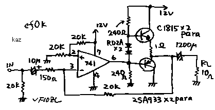
ef0k.gif
Emitter-follower-power-amplifier.
See upper side of the figure! It is called the pure-complementally-push-pull-amplifier. I made it and the maximum power of it was 110mW. See lower side of figure. In this circuit, lower side of totem pole (PNP-transistor) is replaced by the resister. 2SC1815 acts as emitter-follower. Output impedance of this circuit is decided by the Re-resister. Therefore we must use about 8 ohm Re, in order to use 8 ohm speaker. Power-output of this circuit is 72mW. This circuit needs very big idle-current (=150mA), so it is not power-effective. But this machine acts as A-class-amplifier; therefore it has no possibility to make any torsion.
.
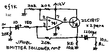
ef1k.gif
 エミッター-
フォロア- パワー-増幅器.
エミッター-
フォロア- パワー-増幅器.
上の図を見て下さい! この回路は,純コンプリメンタルプシュプル増幅器と呼ばれています.これを作ったところ,最大出力110mWが得られました.下側の図を見て下さい.この回路では,トーテムポールの下側(
PNPトランジスター)は,抵抗によって置き替えられています.2SC1815 は,エミッターフォロアとして動作しています.この回路の出力インピーダンスは,Reと書いた抵抗によって決められています.それゆえに,8
オームスピーカーを使うためには,Reに約8 オームを使わなくてはいけません.このサーキットの出力電力は,72mW
です.この回路は,とても大きいアイドル電流( = 150mA ) が必要です,したがって,それは,電源が効率的ではありません.しかし,この機械はAクラス増幅器として動作しています。それゆえに,これは,ひずみを生じる可能性が有りません.
add description on 14 feb 98
追加記載 1998.2.14
ef3.gif
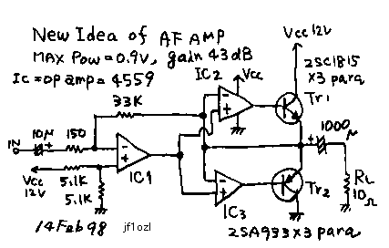
New type of complimentary power amplifier
(It is my idea!)
I will show you my new idea about a complimentary power amplifier. See
the circuit of upside "ef0k"! This circuit has a weak point.
The current of the bias diodes changes, because the voltage on the output
of the driver IC changes. Then the bias voltage has to changes. That makes
a distortion. See the circuit of lower side "ef3"! IC2 and TR1
construct an emitter follower circuit like that of "ef1". IC3
and TR2 also construct an emitter follower. On each circuit, the minus
input of the operational amplifier is connected to the emitter of the transistor;
therefore the emitter's voltage becomes the same voltage from a plus input
of the operational amplifier. Therefore this circuit constructs a linear
current amplifier. The voltage amplification of it is 1 times. IC1 works
as a voltage amplifier. The minus input of it is connected to the output
of the whole circuit. Therefore the whole minus feedback is made by IC1.
The distortion of this circuit is very small. This amplifier has 0.9W power
output. Frequency characteristic is very flat from 333Hz to 24 kHz. It
is my idea. But I am only amateur of electronics. I did not make any survey
about patent of this circuit.
ニュータイプのコンプリメンタリー増幅器(私のアイデアです。)
上の図(EF0K)に示された、良く知られたコンンプリメンタリーパワーアンプを基に、新しい回路を考案したので、紹介します。EF0Kの回路では、トランジスターのバイアス部分に回路上の欠点があります。741ICの6番ピンの電圧が変化すると、二個のバイアスダイオードに流れる電流も変化して、結果的にバイアス電圧が変動してしまいます。上の図では、この影響を軽減するために、二個のダイオードに22mAもの電流を流しています。ここの所にFETを使った定電流回路を使う例も雑誌にみられますが、ちょっとスマートでない。さて、EF3の図をご覧ください。IC2とTR1は、真ん中のEF2の図と同じエミッターフォロアー回路を形成しています。IC3とTR2は同じ回路をPNPトランジスターで作って、電源とアースを逆転した回路です。(正直いって、私も、真空管から入った物ですから、この、PNPトランジスターのマイナスが電源というやつには、まさに天地逆転の感があり、なかなかついていけませんでした。)それぞれの二つのエミッターフォロワー回路は、出力トランジスターのエミッターから、オペアンプのマイナス端子にフィードバックループが形成され
ているので、結果として、エミッタの電位はICのプラス入力端子の電位に等しくなります。よって、IC2とIC3の入力をつないでやると、ここを入力とした、電圧増幅率が1倍の電流増幅器が出来る訳です。あとは、IC1によって、普通の単電源の反転増幅器をつくってやり、これにもう一度全体的な負帰還をかけて、歪みを低減しています。実際に作ってみると、考え通りあっけなく作動しました。実測最大無歪み出力0.9Wと12V電源としては上出来です。なにしろ、この回路には、時定数を持つ部分が入力のコンデンサーくらいしかありませんから、全体がオペアンプみたいなもので、周波数特性は333Hzから、23KHzまで完全にフラットでした。私はデュアルオペアンプのCXA4559P(ソニー製)を二個使いましたが、単電源用のクワッドを使えば、大変スマートに基板化出来ると思います。何しろ無調整で、部品も選びませんから、良い回路だと思いますが、いかがでしょう。
--------------------------------------------------------
I would like for you to put my mail on your home page. I am attaching the
amplifier schematic in gif format this time in hopes that you can read
it. Again, thanks for putting up such a great page. Best Regards, Ray Given
AB0Hz -----Original Message----- From: jf10zl@intio.or.jp [SMTP:jf10zl@intio.or.jp]
Sent: Saturday, December 11, 1999 6:39 AM To: 'Ray Given' Subject: RE:
Dear Ray. Thanks your letter. I want to up your mail on my home page. Please
agree it. Please send me what you send me with gif or bmp! I can not deal
tiff. Kaz ---------- From: Ray Given[SMTP:raygiven@foxinternet.net] Sent:
Saturday, December 11, 1999 5:39 To: 'jf10zl@intio.or.jp'<< (J L'2Y
: Aud_AMP.tiff>>Dear Kazuhiro, (J I want to thank you for putting
up such a wonderful web site. I am a radio amateur and enjoy building equipment
myself. I have spent many wonderful hours looking at your designs and contemplating
my own. I particularly want to thank you for the idea on building an audio
amplifier using a Quad Op Amp and two power transistors. I am attaching
a schematic of my finished amplifier. It will drive a 4 ohm/15watt computer
speaker at 2.5 watts and sounds great. It works extremely well and will
be a standard building block for my future projects needing an audio amplifier.
It also provides one extra Op Amp to do additional filtering if necessary.
The minor circuit changes insured stable operation with out oscillation.
I have attached a copy of the schematic in tif format. 73 Ray Given AB0Hz
ef4.gif
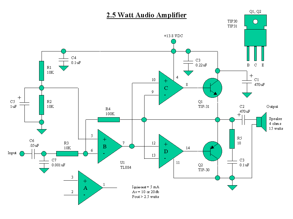
追記:12DEc99:レイさんから、私の回路をアレンジして2。5Wのアンプを作った。快適。とのお便りをいただき、同時に回路図をおよせいただきましたので、上に紹介します。
return to index